- 您现在的位置:买卖IC网 > Sheet目录3832 > PIC16C924-04/L (Microchip Technology)IC MCU OTP 4KX14 LCD DVR 68PLCC
Micrel, Inc.
KSZ8873MLL/FLL/RLL
September 20, 2013
100
Revision 1.6
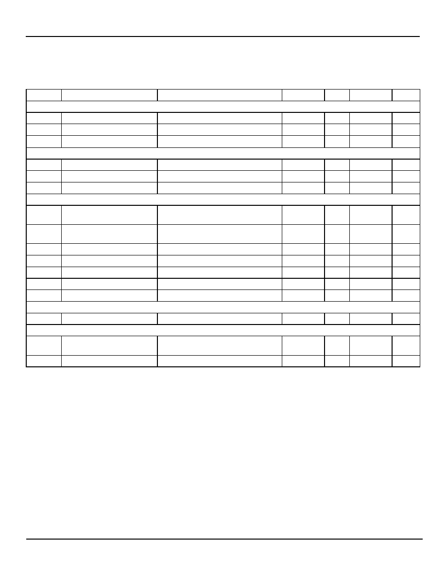
Electrical Characteristics
(10) (Continued)
Current consumption is for the single 3.3V supply device only, and includes the 1.8V supply voltages (VDDA, VDDC) that are provided via
power output Pin 56(VDDCO). Each PHY port’s transformer consumes an additional 45mA @ 3.3V for 100BASE-TX and 70mA @ 3.3V
for 10BASE-T at fully traffic.
Symbol
Parameter
Condition
Min.
Typ.
Max.
Units
CMOS Inputs (VDD_IO = 3.3V/2.5V/1.8V)
VIH
Input High Voltage
2.0/1.8/1.3
V
VIL
Input Low Voltage
0.8/0.7/0.5
V
IIN
Input Current
VIN = GND ~ VDD_IO
10
A
CMOS Outputs (VDD_IO = 3.3V/2.5V/1.8V)
VOH
Output High Voltage
IOH = -8mA
2.4/2.0/1.5
V
VOL
Output Low Voltage
IOL = 8mA
0.4/0.4/0.3
V
|IOZ|
Output Tri-State Leakage
10
A
100BASE-TX Transmit (Measured Differentially After 1:1 Transformer)
VO
Peak Differential Output
Voltage
100 termination across differential
output
0.95
1.05
V
VIMB
Output Voltage Imbalance
100 termination across differential
output
2
%
Tr/Tf
Rise/Fall Time
3
5
ns
Rise/Fall Time Imbalance
0
0.5
ns
Duty Cycle Distortion
±0.5
ns
Overshoot
5
%
Output Jitter
Peak-to-peak
0.7
1.4
ns
10BASE-T Receive
VSQ
Squelch Threshold
5MHz square wave
400
mV
10BASE-T Transmit (Measured Differentially After 1:1 Transformer)
VP
Peak Differential Output
Voltage
100 termination across differential
output
2.4
V
Output Jitter
Peak-to-peak
1.4
11
ns
发布紧急采购,3分钟左右您将得到回复。
相关PDF资料
PIC16F767-I/SO
IC PIC MCU FLASH 8KX14 28SOIC
PIC24FJ64GA310-I/PF
MCU 16BIT 64KB FLASH 100TQFP
DSPIC33FJ64GP202-E/MM
IC DSPIC MCU/DSP 64K 28-QFN
PIC16F876A-I/ML
IC MCU FLASH 8KX14 A/D 28QFN
PIC16F876A-I/SO
IC MCU FLASH 8KX14 EE 28SOIC
PIC16F876A-I/SP
IC MCU FLASH 8KX14 EE 28DIP
AT87C51RD2-3CSUM
IC 8051 MCU 64K OTP 40MHZ 40DIP
DSPIC33FJ64MC802-I/SO
IC DSPIC MCU/DSP 64K 28-SOIC
相关代理商/技术参数
PIC16C924-04/PT
功能描述:8位微控制器 -MCU 7KB 176 RAM 52 I/O RoHS:否 制造商:Silicon Labs 核心:8051 处理器系列:C8051F39x 数据总线宽度:8 bit 最大时钟频率:50 MHz 程序存储器大小:16 KB 数据 RAM 大小:1 KB 片上 ADC:Yes 工作电源电压:1.8 V to 3.6 V 工作温度范围:- 40 C to + 105 C 封装 / 箱体:QFN-20 安装风格:SMD/SMT
PIC16C924-04I/L
功能描述:8位微控制器 -MCU 7KB 176 RAM 52 I/O RoHS:否 制造商:Silicon Labs 核心:8051 处理器系列:C8051F39x 数据总线宽度:8 bit 最大时钟频率:50 MHz 程序存储器大小:16 KB 数据 RAM 大小:1 KB 片上 ADC:Yes 工作电源电压:1.8 V to 3.6 V 工作温度范围:- 40 C to + 105 C 封装 / 箱体:QFN-20 安装风格:SMD/SMT
PIC16C924-04I/PT
功能描述:8位微控制器 -MCU 7KB 176 RAM 52 I/O RoHS:否 制造商:Silicon Labs 核心:8051 处理器系列:C8051F39x 数据总线宽度:8 bit 最大时钟频率:50 MHz 程序存储器大小:16 KB 数据 RAM 大小:1 KB 片上 ADC:Yes 工作电源电压:1.8 V to 3.6 V 工作温度范围:- 40 C to + 105 C 封装 / 箱体:QFN-20 安装风格:SMD/SMT
PIC16C924-08/L
功能描述:8位微控制器 -MCU 7KB 176 RAM 52 I/O RoHS:否 制造商:Silicon Labs 核心:8051 处理器系列:C8051F39x 数据总线宽度:8 bit 最大时钟频率:50 MHz 程序存储器大小:16 KB 数据 RAM 大小:1 KB 片上 ADC:Yes 工作电源电压:1.8 V to 3.6 V 工作温度范围:- 40 C to + 105 C 封装 / 箱体:QFN-20 安装风格:SMD/SMT
PIC16C924-08/PT
功能描述:8位微控制器 -MCU 7KB 176 RAM 52 I/O RoHS:否 制造商:Silicon Labs 核心:8051 处理器系列:C8051F39x 数据总线宽度:8 bit 最大时钟频率:50 MHz 程序存储器大小:16 KB 数据 RAM 大小:1 KB 片上 ADC:Yes 工作电源电压:1.8 V to 3.6 V 工作温度范围:- 40 C to + 105 C 封装 / 箱体:QFN-20 安装风格:SMD/SMT
PIC16C924-08I/L
功能描述:8位微控制器 -MCU 7KB 176 RAM 52 I/O RoHS:否 制造商:Silicon Labs 核心:8051 处理器系列:C8051F39x 数据总线宽度:8 bit 最大时钟频率:50 MHz 程序存储器大小:16 KB 数据 RAM 大小:1 KB 片上 ADC:Yes 工作电源电压:1.8 V to 3.6 V 工作温度范围:- 40 C to + 105 C 封装 / 箱体:QFN-20 安装风格:SMD/SMT
PIC16C924-08I/PT
功能描述:8位微控制器 -MCU 7KB 176 RAM 52 I/O RoHS:否 制造商:Silicon Labs 核心:8051 处理器系列:C8051F39x 数据总线宽度:8 bit 最大时钟频率:50 MHz 程序存储器大小:16 KB 数据 RAM 大小:1 KB 片上 ADC:Yes 工作电源电压:1.8 V to 3.6 V 工作温度范围:- 40 C to + 105 C 封装 / 箱体:QFN-20 安装风格:SMD/SMT
PIC16C924CL
制造商:MICROCHIP 功能描述:New